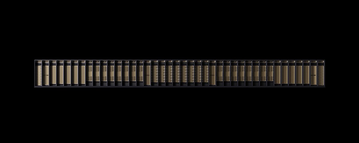
In August I wrote that the scarce resource in AI was no longer the GPU but the DRAM die and the substation. The market at that moment was punishing capital spending. It has since stopped. Nvidia's August quarter and Oracle's September quarter both got rewarded, and the 2027 spending forecasts nearly doubled.
That reversal looks irrational if you only read the balance sheets. It looks different if you read the hardware. What follows is the technology layer underneath the money — because the constraints that matter now are physical, and they are the reason the spending keeps going up rather than down.
1. Rubin is not a chip refresh. It's a data center redesign.
Nvidia’s Vera Rubin platform is now ramping into full production, with production shipments set to begin this fall. The specs are impressive on their own: 50 PFLOPS of NVFP4 inference per package, five times Blackwell, with 288 GB of HBM4 at 22 TB/s — a bandwidth figure Nvidia raised from its original 13 TB/s target. The Vera CPU brings 88 custom Arm cores. NVLink 6 doubles per-GPU scale-up bandwidth to 3.6 TB/s, and ConnectX-9 doubles the scale-out NIC to 1.6 Tb/s.
But the number that reshapes the industry isn't a FLOPS figure. It's the power envelope.
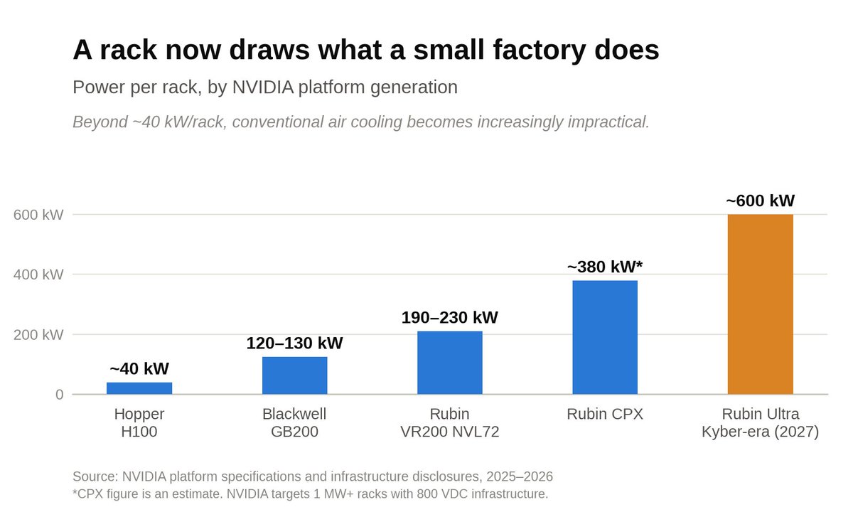
A VR200 NVL72 rack draws roughly 190–230 kW, up from 120–130 kW for Blackwell and around 40 kW for Hopper. The 2027 Rubin Ultra "Kyber" rack, housing 576 GPUs, is specified at roughly 600 kW, with 1 MW-class racks behind it. The CPX variant aimed at long-context prefill lands at around 370 kW on its own.
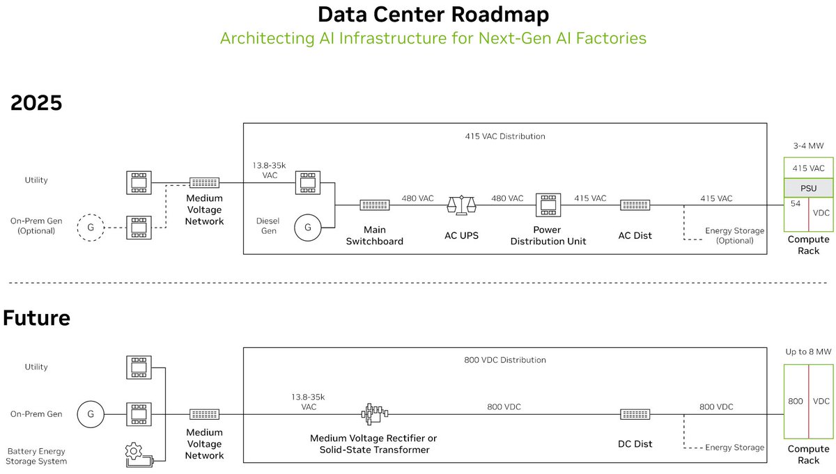
This forces a wholesale change in how buildings are wired. Nvidia is moving the industry toward 800-volt DC distribution, replacing traditional 415 or 480 VAC three-phase systems. At the row level, Nvidia says 800VDC can transmit 85% more power through the same conductor size while reducing copper requirements by 45% compared with 415 VAC distribution. The NVL144 rack design uses 45°C liquid cooling, a liquid-cooled busbar, twenty times more onboard energy storage to hold voltage steady, and a central PCB midplane replacing cable harnesses.
Here is the part operators keep underestimating. Racks refresh roughly every three years. Buildings do not. If your facility was designed around a 72-GPU NVLink domain and 130 kW per rack, the next platform doesn't fit — and retrofitting costs far more than designing ahead. That is the stranded-asset problem sitting quietly underneath the capex numbers, and it is one reason spending accelerates rather than flattens: a large share of the buildout isn't incremental capacity, it's replacing halls that became obsolete faster than they depreciated.
2. The real bottleneck is the package, not the transistor
This is the least understood part of the cycle, and the most important.
A gate-all-around transistor on N2 or Intel 18A is a transistor. An EUV scanner is a patterning tool. Neither of them attaches eight HBM stacks to two reticle-sized GPU dies. The 2026 volume AI accelerator is still mostly FinFET logic plus HBM plus a 2.5D package — and the package is the long pole.
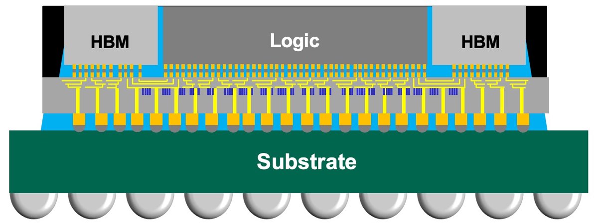
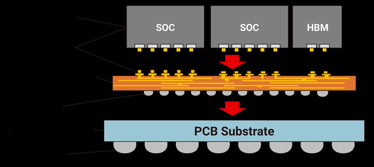
TSMC's C.C. Wei said so publicly on the July 16 earnings call, answering a question about competing advanced-packaging supply: "our packaging capacity is so tight that now it limits my customers' growth." Read that carefully. The world's largest foundry is telling you that front-end wafers are piling up behind the back end.
The capacity math backs it up. CoWoS is expected to reach roughly 115,000–140,000 wafers per month by the end of 2026, rising to around 170,000 in 2027, with expansion concentrated in Tainan and Chiayi. Nvidia has reportedly booked over half of TSMC's 2026 CoWoS capacity. Meanwhile N2 and A16 fabs are booked well into 2028, with lead times measured in the 78–156 week range.
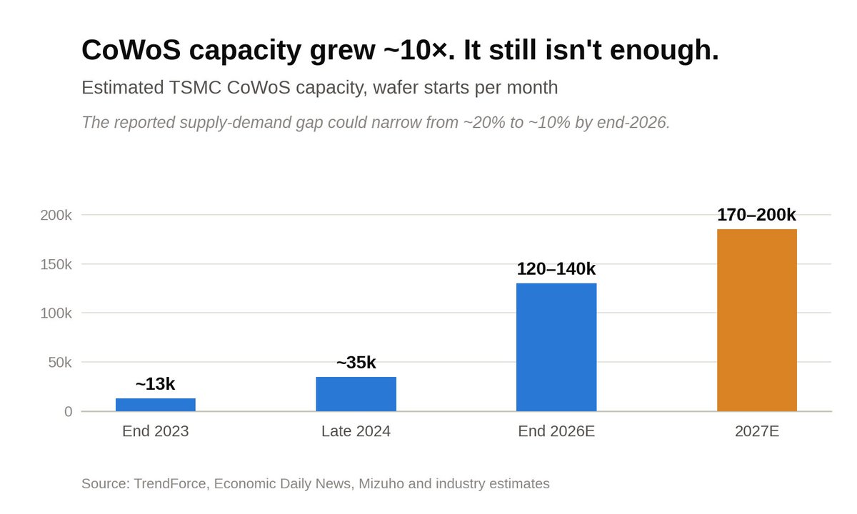
The workaround paths are all mid-maturity. TSMC is pushing CoPoS panel-level packaging, piloting fan-out panel processes at Chiayi, where rectangular panels replace round 12-inch wafers for better area utilization. Glass-core substrates are a cost-down alternative that Wei described as needing roughly another year on a pilot line before production. Intel's EMIB and Foveros are being evaluated as overflow, as are Samsung's I-Cube and X-Cube and Amkor's OSAT lines — all at lower throughput with their own 26–39 week lead times.
For anyone planning silicon: a front-end wafer slot without a matching packaging slot does not ship. That sentence is the whole 2026 supply chain in one line.
3. Memory: two markets that stopped being one
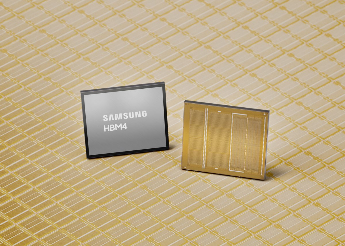
On the leading edge, HBM4 is ramping hard. Micron is adding up to 60,000 HBM wafers per month to reach roughly 100,000 by year-end, with 12-high HBM4 for Vera Rubin potentially half its output, against Samsung and SK hynix at roughly 150,000–200,000 each. Samsung's HBM share could approach 40% in Q4 from 33% in Q2; SK hynix holds around 50%. HBM4 brings a 2048-bit interface and 16-high stacks, which raises yield and thermal risk in exactly the way hybrid bonding was invented to solve.
On the commodity side, the squeeze got worse, not better. TrendForce raised its Q3 PC DRAM forecast from 8–13% to 15–20% and Q4 from 0–5% to 3–8%, with server DRAM up 13–18% in Q3. The benchmark DDR4 spot chip hit a record $42.50 in early August. Citi models enterprise 64GB DDR5 RDIMM going from $873 in Q1 to roughly $1,586 by Q4. Apacer's CEO expects severe shortage into at least mid-2027.
These are the same fabs. Every wafer converted to HBM for an AI server is a wafer not making the DRAM in a laptop — at roughly a 3-to-1 conversion ratio. And the relief valve is years out: new Samsung and SK hynix fabs don't ramp before H2 2027, and Micron's first new US fab in Idaho doesn't start DRAM production until mid-2027.
4. Optics crossed the line from research to production
The quieter technology story of 2026 is that copper ran out of road and the industry had an answer ready.
Co-packaged optics puts the optical engine in the same package as the switch ASIC, collapsing the electrical path.
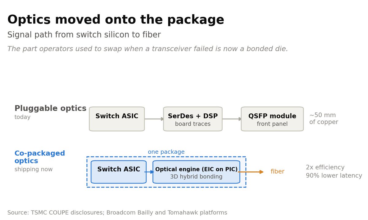
Nvidia's numbers for CPO versus pluggable modules: roughly 3.5x better power efficiency, 64x better signal integrity, 10x resilience from fewer active devices, and about 30% faster deployment. The company has been explicit that this is a structural requirement for next-generation AI data centers rather than an optional upgrade.
Both Nvidia and Broadcom have moved CPO into initial production for scale-out switches, with scale-up deployment targeted for 2027–28.
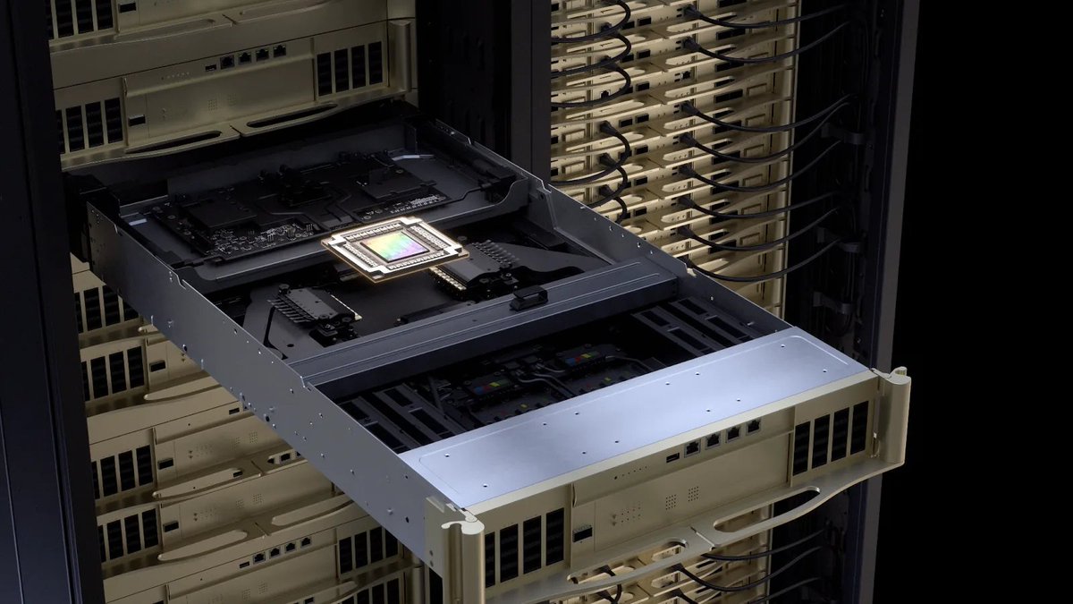
Both build on TSMC's COUPE platform, which stacks a 65nm electronic IC with a photonic IC using SoIC-X, and whose roadmap runs 1.6 Tb/s for OSFP connectors, then 6.4 Tb/s co-packaged in CoWoS, then 12.8 Tb/s in-processor. Broadcom's third-generation CPO runs 200 Gb/s per lane with a fourth generation at 400 Gb/s in development. At OFC in March, Ayar Labs and Wiwynn showed a complete scale-up rack with 100% CPO interconnect.
Nvidia's own framing is the tell: most of a system's bandwidth is now concentrated at the scale-up layer. That is where the optics has to go next, and it's why TSMC is folding COUPE directly into CoWoS — the packaging constraint and the optics roadmap are now the same constraint.
5. What this does to the financial picture
Now the money makes sense.
Nvidia reported $96.2 billion in revenue on August 26, up 106% year over year, with 75% gross margin and October-quarter guidance implying 89% growth — at a 74% margin that now visibly absorbs memory cost inflation. Oracle followed on September 10 with $664 billion in remaining performance obligations, up $209 billion year over year, cloud infrastructure revenue up 121%, and roughly $5 billion of negative free cash flow while delivering 850 MW of capacity in a single quarter.
The forecasts moved with them. Nvidia's CFO said top-five hyperscaler capex goes from about $800 billion in 2026 to $1.3 trillion in 2027, disclosed alongside an Amazon commitment to 2 million GPUs. BofA sees more than $1.2 trillion over the next twelve months, against a roughly $700 billion consensus earlier in the summer. UBS models $1.009 trillion in 2026, $1.447 trillion in 2027 and $1.619 trillion in 2028 — with Amazon, Alphabet and Microsoft spending 102% of cloud revenue on capex this year. S&P Global Ratings expects all six hyperscalers in its analysis to generate negative free operating cash flow in both 2026 and 2027, with recovery not projected until 2029.
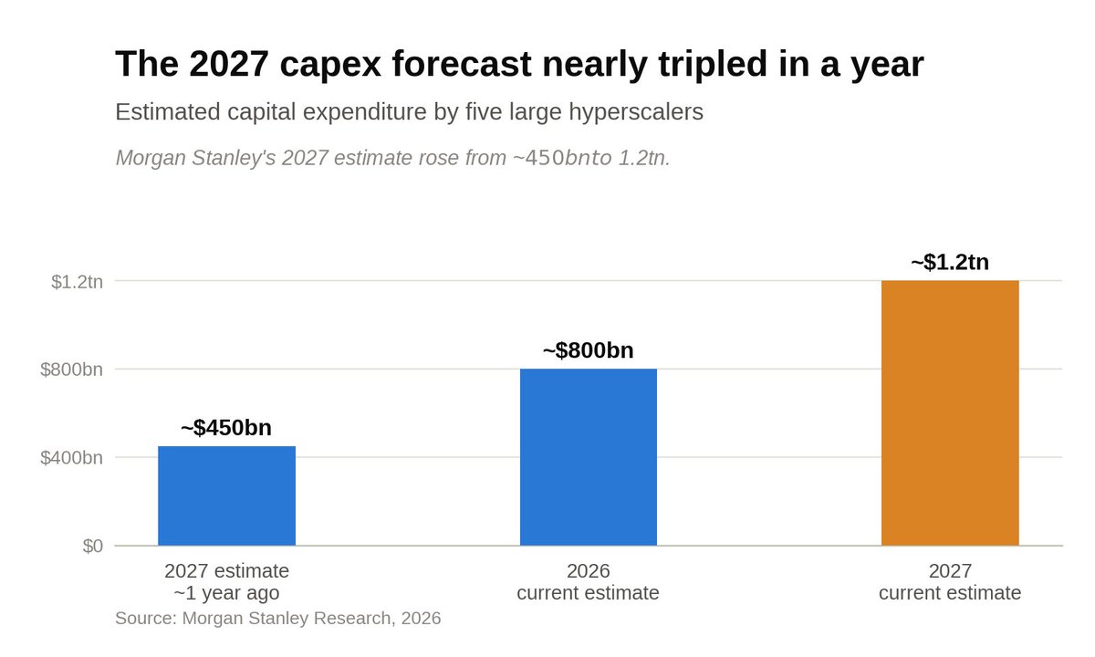
Two counterweights are worth holding onto. Nvidia has beaten its own guidance thirteen quarters running, but the beat has compressed from +22.8% to +4.6% — the earliest signal that supply is catching demand. And FERC's June order now requires data centers to pay the full cost of grid upgrades tied to their own interconnection, in a country where electricity costs are up 42% since 2019. The next binding constraint may be a state legislature rather than a transformer.
What I'd watch
Packaging capacity, not wafer capacity. CoWoS and CoPoS ramp rates tell you more about 2027 accelerator supply than any node announcement.
Whether 800VDC and CPO land on schedule. Both are prerequisites for the Kyber generation. Slippage in either pushes the compute curve right regardless of how much money is available.
The compressing beat. Another sub-5% quarter from Nvidia in November would say more than the headline number.
The thing that has actually changed since August is the nature of the question. In July people asked whether the spending would stop. In September the question is whether anyone can physically build fast enough to absorb $1.3 trillion — through a packaging line that its own CEO says is capping customer growth, a memory market that can't add cleanrooms before late 2027, and a grid whose regulator just moved the bill.
This piece builds on my earlier analysis of the 2026 hardware cycle, The Bottleneck Moved, while also reflecting some of what I’m seeing firsthand while building Ateno. I’ll publish a further update later this fall, once the October-quarter results and GTC roadmap disclosures are in. Together, those should resolve several of the open questions above—and provide a clearer picture of where the industry is actually heading.